True Bypass For Boss (without ruining the box!)

15 04 2009

Greetings,
Many people are hot on the “True Bypass” thing. The electronic switching as used by Boss, Ibanez, and many other popular effects is considered passé, as now people want to have their bypassed signal completely un-tainted by superfluous buffers. And in some cases they have a valid point, if you have 6 Boss pedals all strung together, your signal is going through as many as 12 buffers, and in the case of the transistor emitter-follower type as is used in these pedals (which always has slightly less than unity gain), this can result in a substantial signal loss.

So, it has become popular to modify these effects to have mechanical switches that fully bypass the signal when the effect is turned off. There is one big problem; most people seem to think the best choice of switch is the large 3PDT footswitch sold by New Sensor (or Cliff, or Fulltone…) that is popular in many DIY and boutique builds. This is generally a good quality switch, but it is LARGE, and there isn’t adequate space in the Boss Compact series case design to accommodate it. In fact, the Boss case is designed to have a large actuation plate pressing on a very small switch, so there is no space at all for anything but a very small switch. In an attempt to make the large switches fit, there have been countless examples of the attractive and functional appearance of pedal ruined by drilling holes through the actuator plate to fit the switch. You’ve seen them… these ugly things with huge footswitches sticking out of them… terrible.

But there is an elegant solution to this problem, and it’s actually quite simple – just use a small mechanical DPDT pushbutton switch that fits correctly under the actuator. You can see one here:

True Bypass in an old Boss BF-2

True Bypass in an old Boss BF-2


The only trick is to get the height of the switch plunger adjusted so that the actuator presses on it correctly. Foam rubber makes this easy.
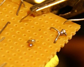
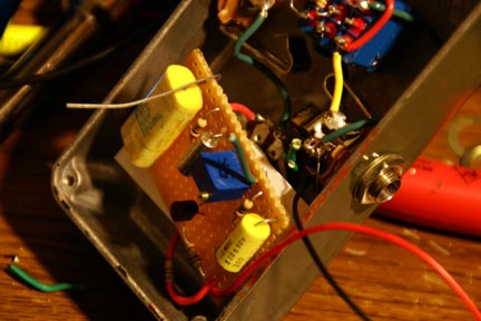
I etched a board to hold the switch and simplify connections. It is held in place by a bolt which is mounted through the stud that holds the actuator spring.
Bypass board for Boss Pedals

Bypass board for Boss Pedals


You can see a tutorial which describes using a small switch like this at Small Bear Electonics (and yes, they sell a similar switch). http://www.smallbearelec.com/HowTos/Shell/Shell.html
For switching the LED, I am using R.G. Keen’s brilliant Millenium Bypass circuit. You can read about that here: http://www.geofex.com/Article_Folders/Millenium/millen.htm
That’s it, very simple really – there is absolutely no reason to hack up a Boss pedal to put true bypass in it. And doing it this way retains much of the “soft” feeling that makes Boss’ Compact pedals such a great design.

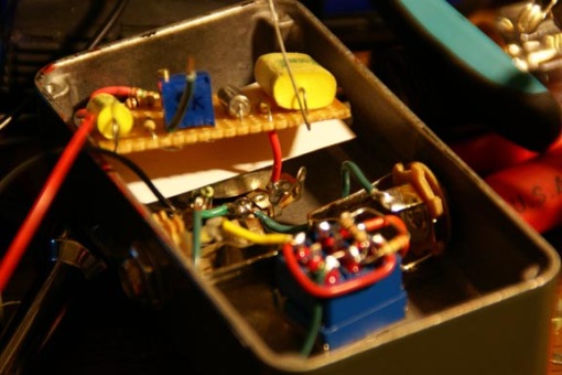
And as for the rest of this old BF-2? I did a handful of simple mods to help to improve it. Firstly, I removed elements of the old switching circuit to accommodate the new mechanical bypass circuit. Then, I replaced the old worn-out electrolytic caps and upgraded them with better types. I also replaced the signal opamps with better low-noise types. The stock 4558s are fine for an old Tube Screamer, but they’re pretty lousy if you want a nice hi-fi sound. Some the two 1uF electrolytics in the signal path were replaced with Nichicon MUSE audiophile grade bipolar types, and a pair of 220nF caps that were previously electrolytic have been replaced with film types for a definite improvement in fidelity. That’s about all this on needed to get some good improvements and lower the noise a bit.
Here’s a pic:

Modded Boss BF-2

Modded Boss BF-2

I hope this little article gives you some ideas for your own mods to the Boss Compact Series. They’re really fun to work on, and little changes can sometimes go a long way.

-MC


Crackle NOT Okay!

8 01 2009

Recently, the Four Banger became a bit of a small hit at The Gear Page. I’ve gotten a good number of orders and I shall be quite busy for the next few weeks. Thanks!
But…. some people seemed to take issue with my inclusion of the circuit inspired by the ZVex Super Hard-On (the section labeled “S” in the Four Banger). Despite the work I put into designing the Four Banger from scratch, including that simple cheap little thing makes me an unoriginal thief in the eyes of certain people.

Since I’m not interested in having to defend myself against being called a “cloner”, I decided to throw out the SHO entirely and design something new to put in there. It took me about three days of experimenting, but finally I came up with what I desired: a circuit that captures the same sound and response as the SHO without that awful crackling noisy gain control!

Behold!
Here it is, the thing so many DIYers have tried to do, but none have ever accomplished, the Crackle-Free SHO!

Now, I admit, it’s not exactly like the SHO, but your ears will have a very hard time telling the difference! When you look at the gain control, you see that the input impedance of the circuit goes down as gain goes up. This is a key ingredient to the SHO-style high gain sound. The input impedance of the original SHO changes like this too, because of the relationship of the feedback resistance vs. gain. Freestompboxes member “estragon” was kind enough to give an excellent explanation about the change in impedance which I shall quote here:

…the input impedance of the SHO is not 5 Mohm as the popular belief dictates. No, it varies big time with the bias pot. At min gain, the end of the upper 10Meg resistor is tied to an inverted copy of the input voltage, not ground, so overall input impedance actually becomes 3.3Mohm when you do the proper math to find out the equivalent thevenin resistor (this has been verified in the sim as well). As the bias pot is reduced and gain increases, something very convenient happens: the input impedance starts going down, down to 140 kohms at max gain. This certainly helps taming the high frequency resonance of any guitar pickup (around 2-5kHz), thus taming highs and helping to the musicality of the clipping. Again, this is because the upper 10Meg resistor is effectively tied to a voltage source that is an amplified version of the input voltage, and not a simple ground point.

So, I have managed to be able to control both the gain and the input impedance in a way which is analogous to the action of the SHO, but with a new method that doesn’t make noise!

What causes the noise in an original Super Hard-On’s gain control, you may ask? It’s not actually the control itself that’s making the noise – attempts at using top quality low-noise controls have been fruitless – it’s the transistor that makes the noise. What happens is that as the gain control is adjusted, the transistor’s bias changes; and because of this change, it switches on and off momentarily while it stabilizes. The two resistors which connect to the Gate (10M in the SHO, 2M2 in my version) allow the circuit to automatically bias to the center of the voltage swing “window” which it has available. But it doesn’t do this automatically, it takes a moment for it to happen; and in the meantime, the transistor is cutting out and crackling. It’s very interesting to hear if you turn the gain control of an SHO very quickly from minimum to maximum gain; the sound will cut out completely for a second and slowly fade back in… very odd behavior, and hardly something I would consider desirable!

So, now we don’t have to put up with that noise any more, because since my version has the Source at a constant level, there is no crackling, popping, fading, etc… because the bias is constant. Instead of using the ratio of Drain to Source resistance to control gain, my circuit uses the ratio of Gate series resistance to Drain/Gate feedback resistance to control gain – just like how you see in an Inverting Op Amp circuit. It’s just as simple and elegant as Vex’s design… except it’s how he should have done it in the first place so he wouldn’t have had to waste so much time and effort convincing people that a noisy junky-sounding gain control is “Okay”!

Where can you go with this? There are many possibilities for this kind of circuit. Just look at Vex’s product line; a substantial number of his things are just various numbers of SHOs all together. With my circuit, I urge that you try something creative; even if you’re keeping it simple, you can do fun things like add an ultra-high impedance input buffer which would allow you to scale down the values of the gain stage’s Gate resistors and Gain control, so you don’t need to use the high values to get a high input impedance. You’ll see how useful that is if you ever try to find 5M controls to use for a super hi-Z version…. High values of resistance contribute noise as well, so there are many advantages to using a buffer with it.

When I find the time, I will put up a DIY project with a printed circuit board layout you can use for your own experiments. And I reiterate, this is now the boost which is used in my Four Banger in the spot previously inhabited by the SHO.

-MC


Total Sonic Annihilation

22 01 2008

A discussion of the Death By Audio – “Total Sonic Annihilation” recently came up in the Forum. Someone posted up a layout supposed traced from one. The device is a simple feedback looper intended to cause other stompboxes to go into a state of self-oscillation. This is a technique which has been used in the Noise community for many years and it’s nothing new to me. But, looking at the diagramme, there are several things which I would change to help make it a more useful device. I present to you here a more “correct” feedback looper which does exactly the same thing as the DBA Total Sonic Annihilation, but allows for a different type of total bypass of the oscillating device.

My Total Sonic Annihilation1

As you can see, the input of the loop is earthed during bypass, which makes sure that it stops oscillating when you bypass. Otherwise, the oscillations can infest the bypassed signal and cause trouble. Also, an additional small-value resistor has been added to the feedback loop to ensure that the output of the device in the loop doesn’t ever become totally shorted to ground, regardless of the setting of the control pot.

This design is slightly different inasmuch as it bypasses the entire effect. I think the DBA one has it so you are running through the looped effect all the time and the bypass switch just turns the feedback on and off. I can see that, but I was going for a different idea with my design. I will probably post up one like that later on today.


JFET Boost

21 01 2008

Let me present to you this, the first DIY project to be published within this Grimoire, a JFET Boost. The circuit is based on an original design by the Analogguru which I have modified to better suit my tastes and improve the performance. This circuit is very simple and an easy build, therefore, it will be shown here being built on perf board. It should prove to be a valuable tutorial for the novice who would like to try his first project or has never built on perf before.

Here is the schematic: JFET Boost

And the layout: JFET Boost Layout1

Here is the Bill of Materials:

Resistors – All are 1/4 watt Carbon Film type.
R1 = 1K (1,000 Ohms)
R2 = 1M (1,000,000 Ohms)
R3 = 10K
R4 = 100R (100 Ohms)
R5 = 330K
R6 = 150R
R7 = 1K

Coupling Capacitors – All are polyester film/foil type. Minimum rating is 15v.
C1 = 100nF (.1uF)
C2 = 1uF

Polarized Capcitors – Minimum 15v rating, Electrolytic or Tantalum.
C3 = 22uF
C4 = 22uF

Semiconductors
Q1 = 2SK117 JFET (J201 or MPF102 may make an adequate substitute)
D1 = LED, whatever size/color you desire

Variable Resistors – All are Carbon type.
Tr1 = 5K Trimpot
P1 = 5K Linear Taper Potentiometer

Hardware
J1 = Phone Jack, 1/4″ Stereo
J2 = Phone Jack 1/4″ Mono
SW1 = 3PDT Footswitch
B1 = 9v Battery with battery snap.
Suitable Enclosure, such as 1290NS or Hammond 1590B. Drilled and painted as desired.
Knob
Perfboard. Cut to size indicated in layout.
Several lengths of 1/16″ heatshrink tubing; used for insulating component leads.
Have everything you need? Okay, let’s get started…

Step One: Cut the perf board to size, then, following the layout, place the components in the perfboard. Bend the leads over so the parts stay in place while working, as shown here:

LayoutPerf

LayoutPerfRear

Step Two: Begin twisting the leads together to form the paths and connections shown in the layout. Double check against the schematic to make sure all the connections are correct. Solder them in place as you go along and trim neatly.

Twist and solder
Trim

When you’ve finished, the board should look something like this:

Board Soldering Done
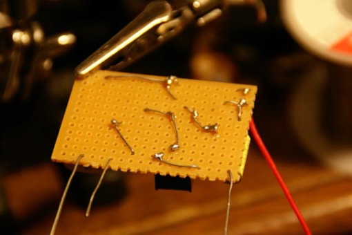
See how the leads to C1, C2, and R4 are left long and free? They will be used to make connections when the board is mounted. It provides a tight, secure connection, and helps hold the board in place.
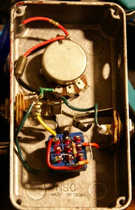
Step 3: Install the hardware and wire up the jacks, control pot, LED, and footswitch. You can see R6 and C4 connected to the LED behind P1. R5 and R7 are mounted directly to the footswitch. When necessary, component leads are insulated with heatshrink tubing.

Wiring

Step 4: Insulate the board from the back of the gain control. The board will be sitting on top of the pot, so it needs to be insulated from it to prevent shorts. I used a piece of card attached with some hot glue. I prefer the hot glue because it’s non-conductive and easy to remove if the control ever needs to be replaced. A more “electrically correct” alternative to the cardstock insulator would be a piece of “fish paper”.

Insulating Card

Step 5: Connect and mount the board. Attach the free end of R6 to its junction point on the board. Then, carefully press the board flat against the back of the control and connect the free end of R4 to the center lug of the control. See it here from a couple angles:

Final Wiring 1Final Wiring 2

Finally, connect the free leads of C1 and C2 to the footswitch. Now we are complete!

Wiring CompleteNow ready for…

Step 6: Calibration. Power up the unit and attach a voltmeter between ground and the junction labeled “Test Point” in the schematic and layout. Adjust Tr1 (Bias trimpot) until the meter reads +5 volts DC as you can see here:

CalibrationThis sets the correct idle current for the JFET and ensures correct operation. Practitioners wanting to live dangerously can experiment with different bias currents to hear what impact it can have on the sound.

Step 7: Enjoy! We are done! You should now have a beautiful and aggressive-sounding JFET Booster. Highly recommended for pushing a crunchy rhythm sound into a saturated lead tone. This device is loud! Please make sure yours isn’t as ugly as mine:

DoneBe kind, I reused a torn up throwaway box. This article is about being pretty on the inside.
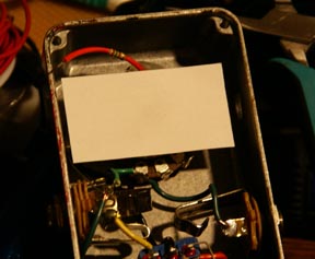
As always, the Master rewards us for our labours. I believe you will be as pleased with this experiment as I. Of course there are innumerable possibilities for modifications, and I may publish some ideas for them as time progresses. In the meantime, I encourage all to share their own ideas and modifications to this highly functional and worthy circuit.

-MC


Voltage Doubler avec MAX1044

21 01 2008

A novitiate practitioner queried concerning the use of a Charge-Pump voltage converter chip as a simple voltage doubler. Here is the formularie of how it is accomplished. The capacitors and diodes are not critical as long as the voltage requirements (at least 24v) are satisfied. The output will be slightly less than double the input because of voltage dropping on the diodes. To minimize this, you can use Schottkey diodes which exhibit a lower voltage drop. Mind the polarity of the capacitors – correct orientation is crucial to success. Care must also be taken that the maximum input voltage of the MAX1044 chip not be exceeded. It can only take a maximum of 10v, so it is recommended that the voltage input (at pin #8) be preceeded by a simple Zener diode voltage regulator. The Zener circuit will provide static discharge protection as well. The MAX1044 (and it’s related cousins) are CMOS devices, and because of this, caution must be used when handling them to avoid damage from electro-static discharge. Unused charge-pump chips must always be stored in a conductive container, such as aluminum foil or an anti-static bag.

Here is the diagramme:

Voltage Doubler

Enjoy,

-M.C.